The next step for electronic noses: overcoming fabrication challenges with nanoprinting
In our previous blog, we introduced the electronic nose, also referred to as e-nose, as a device that combines a sensor array with a pattern recognition algorithm to detect and recognize gases in complex mixtures. The concept is powerful, with exciting potential in fields like environmental monitoring, medical diagnostics, and industrial safety. Despite this promise, e-noses still haven’t made their way into everyday life, and research in the field seems to have lost momentum. We suggest that to truly unlock the potential of this technology, the field needs a fresh push from nanotechnology: one that enables the design of high-performance, reliable, and scalable sensor arrays.
In this article, we examine the sensing materials used in sensor arrays and how they work. We then highlight the key challenges in material manufacturing that continue to hinder the performance of these sensing materials. Finally, we identify how VSParticle’s nanoprinting technology can offer practical solutions, potentially providing the fresh impulse needed to push electronic noses closer to real-world adoption.
Why chemiresistive gas sensors dominate e-nose designs
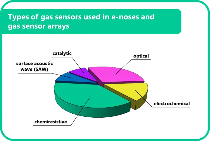
The main workhorses of current e-nose systems are chemiresistive sensors based on metal oxide semiconductors (MOS)(Figure 1) [1]. Their appeal lies in simplicity: their gas sensing mechanism provides a direct, easily measured electrical signal, which maps nicely to compact read-out electronics and integration on MEMS chips. As a result, MOS chemiresistors can be made in a compact size with low cost per unit. Moreover, they are relatively simple to fabricate, sensitive to a wide range of target gases, and offer fast response and recovery times [2].
Working principle of chemiresistive gas sensors: from surface chemistry to signal
Chemiresistive sensors operate based on interactions between gas molecules and the surface of a metal oxide semiconductor (MOS) sensing layer. In a typical MOS-based gas sensor, a layer of sensing material is deposited on the surface of the sensor, while a micro-hotplate is integrated beneath it. The hotplate heats the sensing layer to elevated temperatures needed to enable effective gas adsorption and desorption. In some designs, ultraviolet (UV) illumination can be used as an alternative to thermal activation to trigger the sensing mechanism [3].
When the sensor is exposed to air, oxygen molecules naturally adsorb at the sensing layer’s surface. When the sensing material is an n-type semiconductor (such as the commonly used SnO2, ZnO, or WO3), the adsorbed oxygen captures electrons from the semiconductor’s conduction band to form ionic oxygen species, reducing the free electron population and thus raising electrical resistance. The result is a baseline state that allows the sensor to detect changes when a target gas is introduced.
When the sensor is then exposed to a reducing gas, such as carbon monoxide (CO), hydrogen (H₂), or a volatile organic compound (VOC), the gas reacts with the adsorbed oxygen species on the material surface. This reaction releases the captured electrons back into the conduction band, resulting in a decrease in electrical resistance. Conversely, when the sensor encounters an oxidizing gas, these molecules further deplete electrons from the conduction band, leading to an increase in resistance.
The change in electrical resistance is the core signal used to detect and quantify gas presence. However, the magnitude of this response depends not only on the concentration of the target gas, but also on several other key factors: the operating temperature, the nanostructure and porosity of the sensing layer, and the number of active surface sites available for gas interaction [4].
What’s still holding back sensor performance?
Although chemiresistive sensors are ideal candidates for use in e-noses, turning their promise into consistently high-performing, real-world devices remains difficult, largely due to how the sensing materials are fabricated. A few prominent challenges in MOS sensor fabrication are the following:
Selectivity – While MOS sensors readily detect a wide range of gases, they often struggle to distinguish between them [5]. This cross-sensitivity becomes especially problematic in e-nose systems, where pattern recognition depends on each sensor element responding uniquely to different gas molecules. Without sharper selectivity, MOS-based e-noses fall short of delivering consistent and accurate performance.
Sensitivity – Detecting trace gases at sub-ppm levels is critical in conditions where harmful compounds may be present in tiny amounts. Achieving this level of sensitivity requires materials with high surface area, abundant active sites, and low noise: conditions that are difficult to fulfil using conventional fabrication methods [4].
Stability and reproducibility – Even when fabricated under identical conditions, sensors often exhibit variability in performance, undermining their accuracy in real-world applications. A major challenge in scaling chemiresistive sensors for commercial use as e-noses is ensuring consistent and reliable performance across devices [5].
Scalability and integration – Traditional fabrication techniques involve wet chemistry, binders, or post-processing steps that introduce contamination and are hard to align with MEMS-compatible production [6]. This makes it difficult to integrate MOS sensors effectively into real-world devices while maintaining performance and reliability.
Next-generation manufacturing of sensing layers
The fabrication challenges outlined above highlight a clear gap between the performance potential of MOS chemiresistive sensors and what current fabrication methods can deliver. At VSParticle, we aim to bridge that gap through a novel manufacturing approach that offers precise control over material composition and morphology, while remaining clean, scalable, and reproducible.
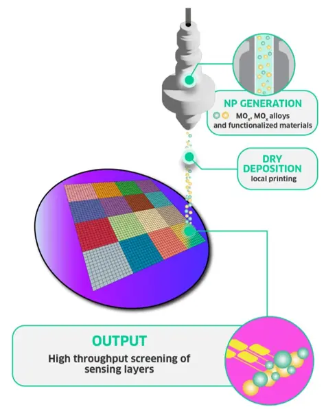
Our technology combines spark ablation with nanoprinting to deposit nanoporous MOS layers with exceptional control (Figure 2). In this dry process, a high voltage is applied
across two conductive electrodes, generating a spark that vaporises electrode material. An inert gas that is flown through the electrode gap rapidly cools the vapor, condensing it into high-purity nanoparticles with tunable sizes (1-20 nm). The nanoparticle aerosol is then directed towards a substrate, onto which it forms nanoporous films or patterns.
The solvent-free approach eliminates the need for wet chemistry, is inherently scalable, and allows for complex patterning on a wide variety of substrates, including sensitive MEMS chips. The following sections detail how this method addresses key challenges in MOS sensor fabrication.
Improved sensitivity through nanoporous layers
Porosity is a critical factor in enhancing the sensitivity of MOS sensors. A porous structure increases the surface area of the sensing layer, providing more active sites for gas molecules to interact with. This results in improved sensor responses, enabling the detection of even trace amounts of target gases. To create such porous structures, scientists commonly use techniques like thermal treatments, template-assisted methods, and solution-based nanoparticle deposition.
VSParticle’s nanoprinting technology takes this a step further by using the smallest stable nanoparticles with sizes <20 nm, produced through spark ablation, to create MOS layers. This approach leads to structures with exceptionally high surface-area-to-volume ratios and significantly lowers the limit of detection (LOD), a key performance metric for gas sensors. A study by Sánchez-Vincente et al. [7] demonstrated that nanoporous ZnO and SnO₂ layers fabricated using spark ablation outperformed those made through conventional methods like drop-casting and electrospray, achieving lower detection limits (sub-ppm) for gases like CO and NO₂.
Compositional fine-tuning for enhanced selectivity
A key challenge in MOS chemiresistive sensors for e-nose technology is achieving the selectivity needed to distinguish between gases in complex mixtures. VSParticle’s nanoprinting technology addresses this challenge by providing unmatched flexibility in material selection and combination. The spark ablation process allows for any conducting material to be used as a nanoparticle source, and up to four different nanoparticle sources can be combined with precise control over their ratio. The technology enables easy exchange of electrodes or adjustment of the nanoparticle sources’ output ratios. This facilitates the systematic exploration of combinations of metal oxides and noble metal dopants, as demonstrated by Sacco et al. [8].
With this material flexibility, the sensing layer composition can be tailored to optimize the detection of specific target gases such as formaldehyde, acetone, or carbon dioxide. By selecting the optimal material combinations, the sensor responses to particular gases can be fine-tuned – without the need to redesign synthesis processes
or re-formulate inks. As a result, sensor designs can be rapidly iterated to optimize performance and achieve the desired selectivity
Clean and uniform layers for reliable gas sensing performance
Reliable sensor performance is crucial for the success of e-nose technologies in real-world applications. VSParticle’s nanoprinting method contributes to this by producing sensing materials with lower noise, a broad linear response across different gas concentrations, and improved repeatability when compared to sensors fabricated using traditional methods [7]. This enhanced reliability and reproducibility make spark ablation-based sensors particularly well-suited for accurate and consistent gas detection in practical environments.
The reliable performance of these sensors is partly due to the highly uniform porous structure of the sensing material, which is consistently reproducible across different devices. Additionally, the surfaces of the sensing materials produced through nanoprinting are ultra-pure, because no solvents or binders are required in the fabrication process. Moreover, by avoiding complex lithography or etching steps, VSParticle’s nanoprinting technology minimizes the risk of contamination and performance variability.
Towards commercial-grade electronic noses
To summarize, VSParticle’s nanoprinting technology offers promising solutions to the fabrication challenges that have hindered the commercialization of e-noses. Lab-scale tests demonstrate the nanoprinting technology as a controlled and reproducible method to produce MOS sensing layers with high porosity, a wide range of material compositions, and complex patterning capabilities. This flexibility enables the creation of sensitive sensing units tailored to detect specific gases, which can be integrated into sensor multiarrays. If these lab-scale advancements can be scaled for mass production, e-nose technologies could finally transition from prototypes to commercially viable products in fields like environmental monitoring, medical diagnostics, industrial safety, and consumer electronics.
References
[1] S.Y. Park, Y. Kim, T. Kim, T.H. Eom, S.Y. Kim, and H.W. Jang. “Chemoresistive materials for electronic nose: Progress, perspectives, and challenges.” InfoMat 1.3 (2019). doi.org/10.1002/inf2.12029
[2] S. Mor, B. Gunay, M. Zanotti, M. Galvani, S. Pagliara, and L. Sangaletti. “Current Opportunities and Trends in the Gas Sensor Market: A Focus on e-Noses and Their Applications in the Food Industry.” Chemosensors 13.5 (2025): 181. doi.org/10.3390/chemosensors13050181
[3] A. Nasriddinov, R. Zairov and M. Rumyantseva. “Light-activated semiconductor gas sensors: pathways to improve sensitivity and reduce energy consumption.” Frontiers in Chemistry 13 (2025). doi.org/10.3389/fchem.2025.1538217
[4] N. Goel, K. Kunal, A. Kushwaha, and M. Kumar. “Metal oxide semiconductors for gas sensing.” Engineering Reports 5(6) (2022). doi.org/10.1002/eng2.12604
[5] A. Rabehi, H. Helal, D. Zappa, and E. Comini. “Advancements and prospects of electronic nose in various applications: a comprehensive review.” Applied Sciences 14(11) (2024): 4506. doi.org/10.3390/app14114506
[6] G. Verma, A. Gokarna, H. Kadiri, K. Nomenyo, G. Lerondel, and A. Gupta. “Multiplexed gas sensor: fabrication strategies, recent progress, and challenges.” ACS Sensors 8(9) (2023): 3320-3337. doi.org/10.1021/acssensors.3c01244
[7] C. Sánchez-Vicente, J.P. Santos, I. Sayago, V. Mazzola, and L. Sacco. “Room-temperature environmental gas detection: performance comparison of nanoparticle-based sensors fabricated by electrospray, drop-casting, and dry printing based on spark ablation.” Chemosensors 13(6) (2025): 219. doi.org/10.3390/chemosensors13060219
[8] L. Sacco, N. Schouten, L. Egger, M. Popov, A. Köck, C. Dösinger, and L. Romaner. “Multiarray gas sensors based on nanoporous layers produced à la carte by spark ablation using metal oxides, binary and ternary alloys”. IEEE Sensors (2024). 10.1109/sensors60989.2024.10785068