Binder-free deposition of nanoporous layers
At VSParticle, we developed an innovative nanoprinting technology to address long-standing challenges in nanoporous material manufacturing. We developed a binder-free nanoprinting technique that enables the deposition of high purity nanoporous layers (NPLs). Eliminating traditional wet chemistry processing steps and offering unmatched material compatibility and precision, the technology pushes the boundaries of performance, flexibility, and scalability across academia and industry.
Unlocking next-generation performance across technologies
Our printed NPLs offer exceptionally high surface areas, making them promising materials to drive improvements in efficiency, sensitivity, and reaction rates across key application areas.
Electrocatalysis
NPLs increase the number of active sites to accelerate reaction rates in CO2RR, N2RR, and more.
Energy storage
NPLs boost charge storage capacity and improve energy efficiency in batteries and supercapacitors.
Gas sensing
NPLs enhance the adsorption of target gases for improved detection sensitivity in next-generation sensors.
Green hydrogen
NPLs reduce loading of scarce materials while maintaining high catalytic efficiency in PEM electrolyzers.
Semiconductors
NPLs enable quantum effects that enhance functionality in electronic devices.
Nanoporous materials from pure elements
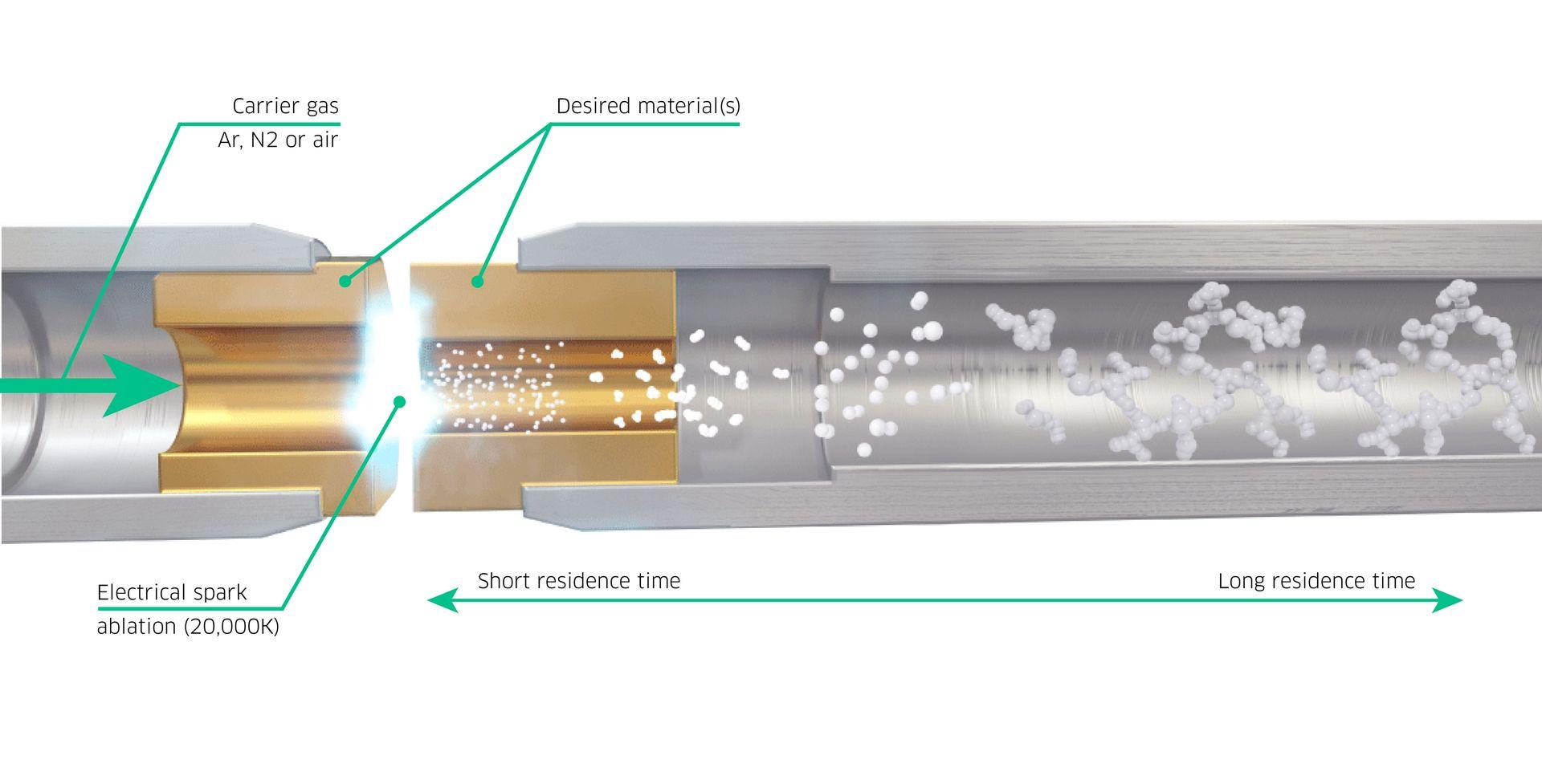
Our nanoprinting technology is based on spark ablation: a dry, purely physical process that only requires electricity, a carrier gas, and electrodes of any conductive material. In this method, a spark locally heats up a source electrode and evaporates atoms from its surface.
When the vaporized atoms enter a stream of inert gas, they rapidly cool and condense to form ultra-pure nanoparticles of 2-20 nm in size. The aerosol is accelerated through a nozzle and printed onto a surface, where the nanoparticles self-assemble to form high-performance nanoporous layers.
Why choose VSParticle's nanoprinting technology?
Scalable from R&D to industrial production
Our technology is inherently scalable: the same nanoporous layer can be reliably reproduced across vastly different scales. We are currently developing an industrial tool to produce nanoporous layers at high volumes, enabling seamless scale-up from small-scale testing to mass-manufacturing.
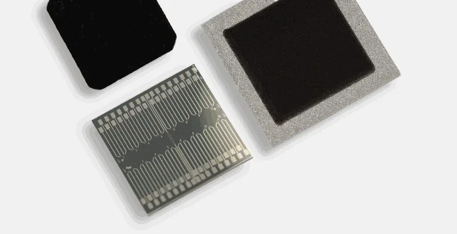
Compatible with any substrate
Because substrate adhesion relies on Van der Waals forces, our technology is substrate-agnostic. Nanoporous layers can be printed onto any flat surface, ranging from Nafion and PTLs to ITO glass, silicon wafers and MEMS chips. It also supports mask-less structuring workflows and enable the direct integration of functional materials into complex device architectures.

Clean and environmentally responsible by design
Unlike traditional chemical synthesis methods, our dry, chemical-free technology yields uncontaminated, binder-free surfaces for optimal performance across application fields. The nanoprinting process is fully powered by electricity, making it a clean and affordable solution with minimal environmental impact.
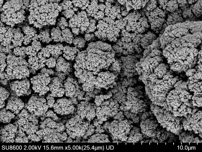
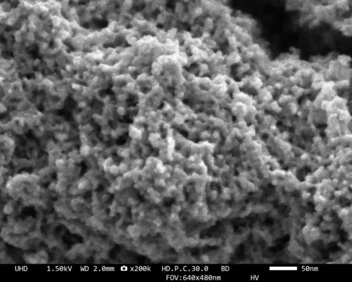
High-surface-area materials
Spark ablation is a synthesis method that naturally self-limits to produce nanoparticles at their smallest stable size, with a narrow size distribution. When these small particles are assembled into layers, they create highly porous films. The high-surface-area structures can unlock enhanced performance across a wide range of applications.

Unique composition flexibility
Our technology is compatible with 40+ elements and can generate a wide range of materials, from pure metals and metal oxides to semiconductors. Multiple source electrodes can be used simultaneously, enabling on-the-fly mixing and engineering of complex composites with tight stoichiometric control. This offers easy access to a myriad of material compositions.
Whether you need unique material compositions, fast validation with
large sample sets, or scalable manufacturing, we help make it possible.
Our products and services
VSParticle manufactures automated tools based on spark ablation technology for nanoparticle synthesis (VSP-G1 Nanoparticle Generator) and deposition (VSP-P1 Nanoprinter). The tools operate at room temperature and ambient pressure and are designed to help our customers in academia and R&D to rapidly unlock materials with unique properties.
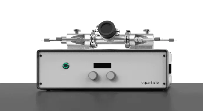
VSP-G1 Nanoparticle Generator
In the VSP-G1 Nanoparticle Generator, a high-voltage electric field between two electrodes causes an electrical spark to form across the gap. This spark locally heats the electrodes to >20,000 °C and ablates atoms from their surface. Upon entering an inert gas stream, usually nitrogen or argon, the atoms cool and condense into nanoparticles. As the nanoparticles are carried away by the gas flow, they may agglomerate and form larger structures. Particle size can be tuned from several atoms to tens of nanometers through the process settings.
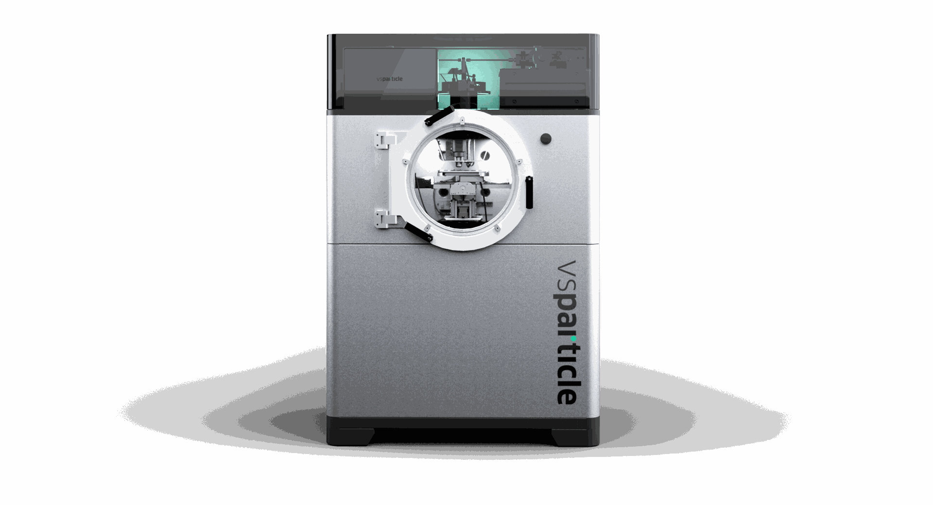
VSP-P1 Nanoprinter
The Nanoparticle Generator can be coupled to a VSP-P1 Nanoprinter for the controlled deposition of the nanoparticles to form nanoporous layers. In the Nanoprinter, the aerosol enters a vacuum chamber and is accelerated to hypersonic speeds through a printing nozzle. The aerosol is directed with a focused trajectory towards a substrate placed on a controlled XYZ-stage. The thickness, porosity, and pattern of the resulting nanoporous layer can be tuned by adjusting the movement of the stage and the operation parameters.
Deposition-as-a-service
We also offer a deposition service in which we utilize our proprietary nanoprinting technology to apply high-quality, uniform nanoporous layers onto the customers’ chosen substrate. The composition and properties of these layers can be tailored to suit specific application requirements in areas such as electrochemistry, catalysis, and sensing. The ready-to-test coated substrates accelerate material selection, layer optimization, and performance validation, helping customers move from concept to results faster.