Tunable nanoparticles and porous thin films for advanced semiconductor manufacturing
As semiconductor manufacturing continues to push into ever smaller dimensions and more advanced packages, the industry faces a critical challenge in detecting, understanding, and eliminating nanoparticles that could compromise device or package yield.
VSParticle offers a dry method for generating and depositing pure or alloyed nanoparticles which helps semiconductor leaders reduce costly yield losses and drive innovation through the application of nanoparticles and porous thin films.
Nanoscale contamination challenge in Semiconductors
The smaller chips get, the bigger the challenge of cleanliness and contamination control. At the frontier of semiconductor scaling, particle contamination, validation of inspection equipment, and cleaning processes become major bottlenecks.
By providing controlled nanoparticles and tunable nanoporous layers, our technology enables R&D and production teams to obtain reliable reference nanomaterials for studying and validating defectivity, cleaning performance, calibration steps, and inspection accuracy, thereby facilitating performance.
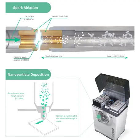
Deposition of metallic nanoparticles for metrology and cleaning validation
VSParticle’s patented spark ablation technology produces and deposits ultra-pure, surfactant-free nanoparticles directly onto any solid substrate, including polymer layers. It can generate particles from over 40 elements and its alloys, maintaining precise size control and surface coverage. This capability enables realistic contamination reference particles, accurate calibration standards, and rapid exploration of new material combinations — all essential for next-generation semiconductor development.
Core capabilities
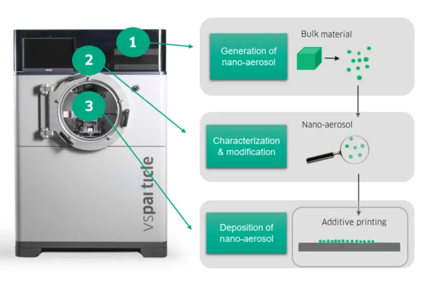
VSParticle's patented technology enables:
- Size selectivity: Pure metallic particles in the range of 2-200nm.
- Material flexibility: Metals, alloys and semi-conductive materials such as Sn, Ni, Au, C, Si and many more.
- Substrate type and size flexibility: Depositions on almost all substrates, from wafers, reticles, pellicles, ceramics to polymers. Flat and non-flat.
- Dry, one-step process: Ligand-free, solvent-free pure particles
- Surface coverage control: From sparse particle
depositions to highly porous thin films.
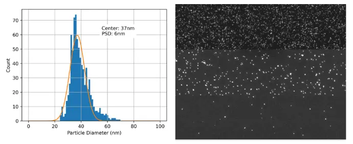
This figure shows typical results obtained with tin particles. We obtained a narrow particle size distribution (PSD) through precise size selection.
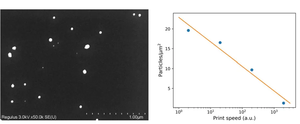
Experimental setup
We control particle coverage on the substrate by adjusting particle generation rate and printer speed. The SEM images show that lower print speeds result in a higher particle density, while increasing the print speed reduces the number of deposited particles.
The graph on the left confirms this inverse relationship between print speed and particle density, illustrating precise, tunable control over surface coverage during deposition.
Creating value across semiconductor applications
VSParticle’s nanotechnology provides a new testing and development platform for the next generation of fabs, equipment makers, and R&D teams — enabling them to explore, validate, and optimize processes at the nanoscale.
Fundamental Research
Provide controlled, pure nanoparticles to model and understand particle behavior under semiconductor-relevant conditions.
Sensing Applications
Enable metal oxide gas sensors with higher sensitivity, greater selectivity, and lower power consumption.
Calibration & Inspection
Generate reproducible nanoparticle to validate and benchmark metrology and inspection systems.
Cleaning & Contamination Control
Replicate realistic nanoscale contamination to test and benchmark particle removal and surface recovery.
Material Exploration
Create nanoporous metallic layers and alloyed structures with tunable properties.
Partner with VSParticle
If you’re tackling challenges in cleanliness, contamination control, calibration, or advanced material development, let’s explore how our technology can accelerate your progress.
📅 Schedule a short call and see where our technology can make the biggest impact in your process.
Our distributors
Tokyo Dylec Corp. (Japan)
1 Naito-cho Building, Naito-cho, Shinjuku-ku
Tokyo, 160-0014 Japan
e: info@tokyo-dylec.co.jp
t: +81 035 367 0891
w: https://www.tokyo-dylec.net
Kyodo International (Japan)
2-10-9, Miyazaki, Miyamae-ku, Kawasaki-shi
Kanagawa-ken, 216-0033 Japan
e: info@kyodo-inc.co.jp
t: +81 044 853 2611
w: https://www.kyodo-inc.co.jp