Optimize your research with highly customizable nanoporous layers
We now offer on-demand nanoporous layer deposition service. Using our patented dry deposition technology, we deposit highly porous, homogeneous layers on substrate of choice to meet your specific application needs.
These ready-to-test coated substrates are ideal for rapid R&D, proof-of-concept validation, and shortening development cycles in a variety of advanced applications, including electrocatalysis (PEMWE, CO₂RR, HER, OER, N₂RR) and gas sensing (CO₂, N₂, CO, NH₃, toluene, H₂).
3
Binder free
The dry manufacturing process generates ultra-pure coatings free of chemical contamination.
3

Low loadings
The reduced loading of coating materials supports both laboratory testing and scalable production.
3
High porosity
The large surface area increases the number of active sites for electrocatalysis or sensing.
3

Uniform thickness
The thickness uniformity of the coated layer facilitates efficient and controlled processes.
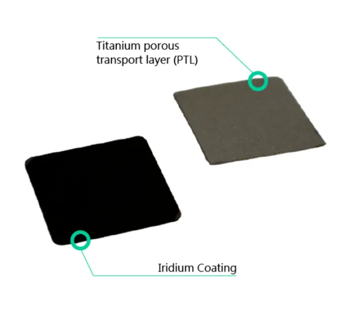
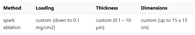
Iridium-coated titanium porous transport layers (PTLs)
Our iridium-coated PTLs are designed for durability in harsh operating conditions. With applications in water electrolysis, N2RR, and CO2RR, the coated PTLs are compatible with both experimental setups and industrial high-current-density environments.
- Customizable loading down to 0.1 mg/cm2
- Flexibility in substrate type and dimensions (up to 15 x 15 cm)
- Large electrochemically active surface area
Thin film coated substrates for electrocatalysis
The electrocatalyst coatings are highly customizable for application in water electrolysis (PEM, AEM, AEL, SOE), fuel cells, CO2RR, N2RR, supercapacitors, ion and redox flow batteries, and other fields.
- Compatible with a wide variety of elements (Pt, Ni, Fe, Cu, and other)
- Ratio-controlled material mixing and alloying
- Coated directly onto the substrate of choice (Nafion, Si, Ti PTL, and other)
Request quote for ECAT coated substrates
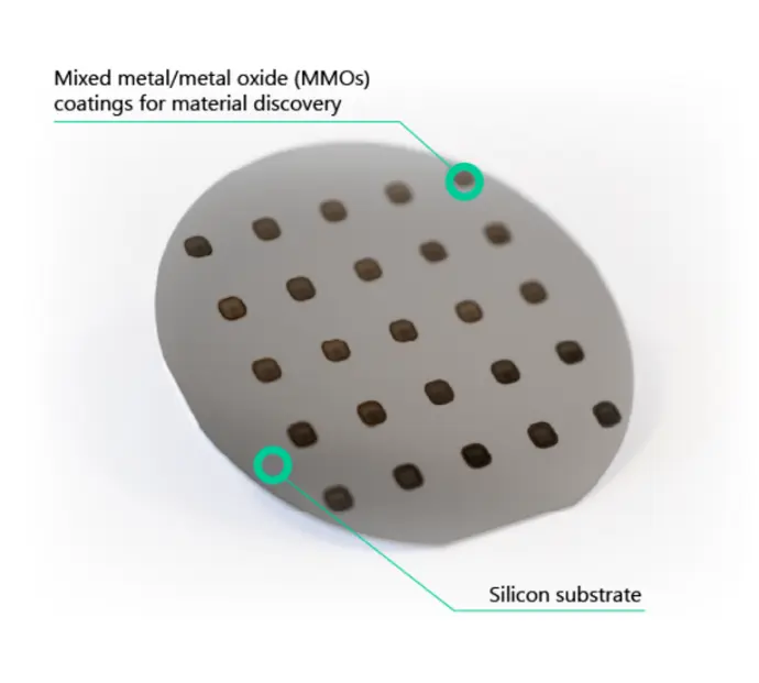
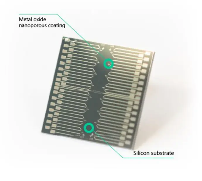
Nanoporous sensing layers on wafers
Custom sensing materials are deposited directly onto your wafer of choice using VSParticle's dry, mask-less printing technology. The sensing layers offer unique material properties to enhance sensing performance and support material optimization processes.
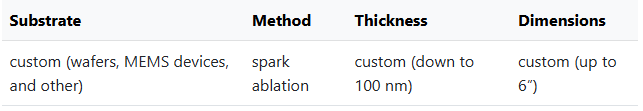
- Ratio-controlled mixing of metal oxides (ZnO, SnO2, NiO, and other)
- High surface area for an improved figure of merit (FOM)
- Mask-less and dry fabrication of multiarrays
Submit request for coated wafers