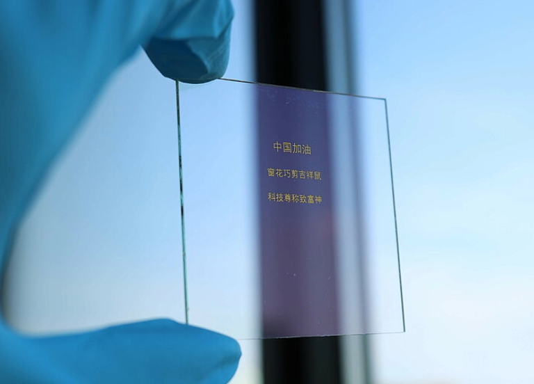
This new way of additive manufacturing can greatly simplify the production of nanoporous thin films and layers with a high surface-to-volume ratio. The applications of such films are numerous and include for example electrocatalysis, chemical, optical or biological sensing as well as the fabrication of batteries and microelectronics.
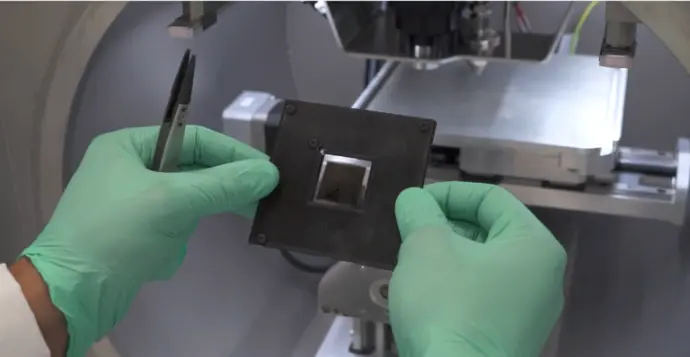
The VSP-P1 Nanoprinter enables you to locally print inorganic nanostructured materials with unique properties. The building blocks for the printed layer are gas-phase produced, sub-20 nm nanoparticles, free of surfactants or any other organic impurities. With the VSP-P1 Nanoprinter, semi-automated printing of nano porous layers of different composition and/or layer thicknesses is possible. Check out our Applications for inspiring examples!
Aerodynamic size 0-300nm particle size: 0-20nm

Any (semi) conductive material

Stable & reproducible

Quick & easy-to-use

Based on spark ablation technology

Clean process: no surfactants or precursors
No handeling of nanoparticels
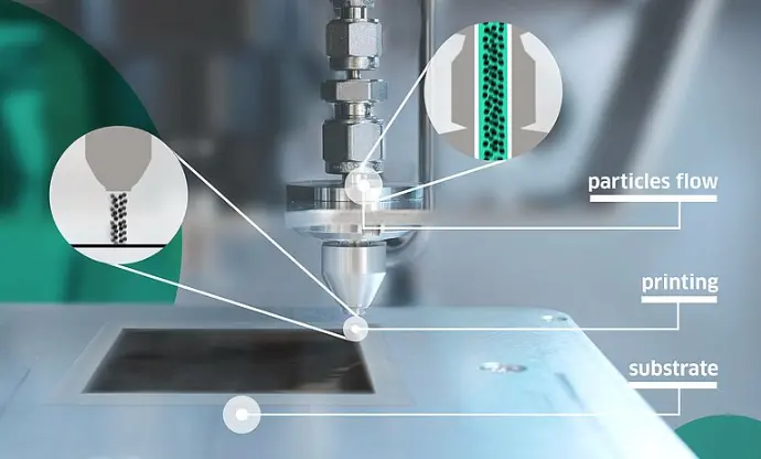
The VSP-P1 Nanoprinter combines generation, combination and deposition of nanoparticles in one automated process, enabling you to print new nanoscale materials without handling nanoparticles. The complete system is operated through a secure and intuitive web interface that allows for automated material production.
Benefits of additive manufacturing
The ability to locally deposit nanoporous thin films with a high surface-to-volume ratio in an additive manner greatly simplifies the manufacturing of materials for various applications (e.g. chemical, optical and biosensing, electro/photocatalysts and electrode materials (e.g. for micro-batteries or bio-electronics).
Process control parameters
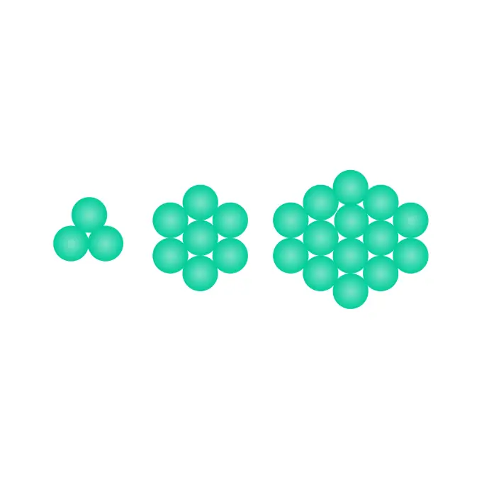
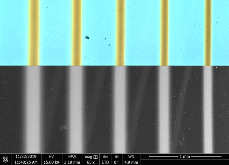
Different layer thicknesses from sparse agglomerates to continuous layers up to a few microns thick are possible using the VSP-P1. The parameters that impact the layer thickness are:
- Nozzle distance to substrate
- Power of ablation
- Printing speed
You can determine the desired printing pattern by running a script through the user interface. Both complex patterns and in-series production of more than one samples are possible using different or modified scripts.
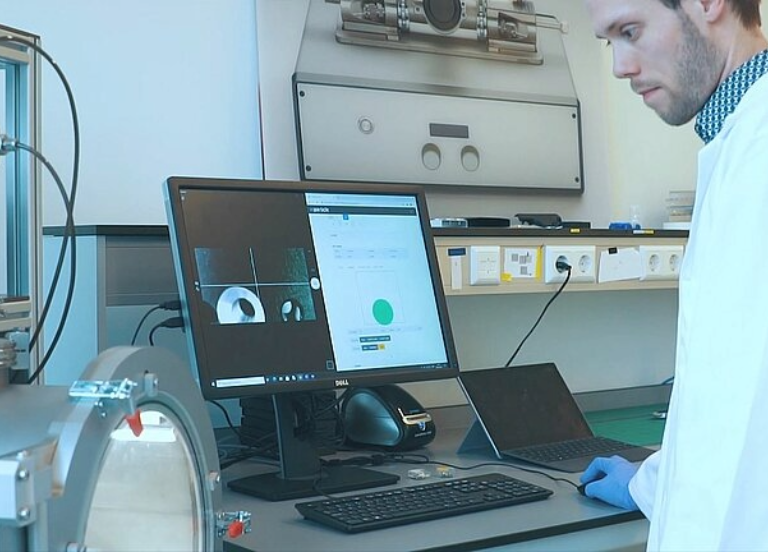
The VSP-P1 NanoPrinter can be controlled directly through the on-device touchscreen, as well as remotely through the hybrid control interface accessible from any device with an internet connection.
VSP-P1 Nanoprinter introduces the most advanced CCM Production
Development of efficient catalyst coated membranes (CCMs) is crucial for the transition towards a hydrogen-based, low carbon economy. Conventional CCM production processes require multiple steps and high loadings of scarce metals. To tackle this challenge, VSParticle introduces membranes. By combining spark ablation, a vapor-based nanoparticle synthesis method, with additive manufacturing, production process of CCMs is simplified and catalyst loading is reduced without compromising performance or durability.